Odawara is located about one hour from central Tokyo in southwest Kanagawa prefecture, and here you can find the Hitachi, Ltd., IT Platform Division Group Odawara Office. This office started out as a plant specializing in computer peripherals in 1966, but its operations now include the development and manufacture of storage systems as well as the design and production of circuit boards.
Hitachi Odawara Office
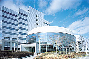
![Odawara Office [Kozu District]](/storage/2014/01/21/cfccb9d2ed62479ac0f7edf552d7b172/35042814_02.jpg)
Odawara Office [Kozu District]
Hitachi produces its storage systems in Oklahoma (USA), Orléans (France), and Odawara, but it installs all components on its PCBAs (Printed Circuit Board Assemblies) at the Odawara Office. Circuit boards are at the heart of computer hardware, so by manufacturing them in one location Hitachi is able to maintain quality at a uniform level and can solve any problems with a single stroke.
Hitachi has established a rigorous set of quality standards for its hardware, including product testing that occupies around 90% of the manufacturing period. ZDNet Japan visited Hitachi's Odawara Office to learn about Hitachi's focus on quality for its hardware products and to see how the products are manufactured. The processes described here are for storage systems, but Hitachi also manufactures its servers in the same manner.
Focus on quality begins at the design stage
Hitachi's focus on quality begins at the product design stage. An example of this can be found in the fact that Hitachi designs with cooling in mind by incorporating temperature management technology that prevent temperature increases to maintain the temperature of their products at an appropriate level during operation and to decrease failure rate. Also, in the unlikely event of a failure in the power module or cooling fans, redundant design ensures that cooling fans and other components are duplexed to enable their replacement without interruption to customer operations.
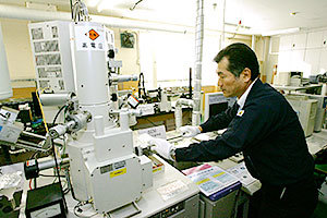
Chemical laboratory
Nanometer-level inspections are carried out at the development stage to ensure component quality. A chemical laboratory has been established in the office for component inspection purposes in order to perform analysis of elements and organic compounds. As well as using a digital microscope and an SEM (Scanning Electron Microscope) to observe shape, surface phenomena, and color, an EDX (Energy Dispersive X-ray) is used to identify elements. Organic compounds such as plastics are analyzed using FT-IR (Fourier Transform Infra-Red) spectroscopy. The devices used have a high level of precision that you would expect to find in research institutes and other such places. At this stage, a load is also applied to components and a lifespan inspection is performed, and components that don't pass this test are never included in products. This chemical laboratory is also sometimes used to investigate failures that occur after delivery to a customer. Component certification in the development stage and a thorough investigation into the cause of any fault is a uniquely Hitachi initiative.
A range of methods for streamlining
Next, we went onsite to see the production area. Yoichi Yamakawa, Manager of the Promotion Center of the IT Platform Division Group of Hitachi, Ltd., Information & Telecommunication Systems Company, showed us around the plant.
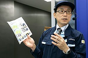
Yoichi Yamakawa
Promotion Center Manager
IT Platform Division Group
Hitachi, Ltd., Information & Telecommunication Systems Company
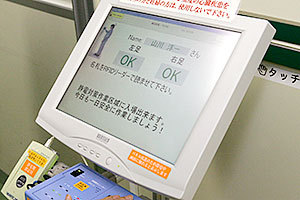
Before entering the production area a machine checks if you're OK in terms of static electricity countermeasures
This plant now uses a method called "rabbit chase production" where a single worker performs multiple processes in sequence. Previously a method where each process was overseen by an individual worker called the relay method was used, but Yamakawa says that "with the relay method you need a person for each process, whereas with the rabbit chase method then there is no idle time and you can easily allocate the appropriate number of staff depending on the volume of production." This means that more efficient use can be made of human resources during production.
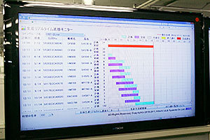
Real time progress monitoring: instant confirmation of any delay via a monitor
The details of operations are visualized with a monitor to enable real time progress checks, so this enables all employees to understand the situation if there is ever a delay. Efforts have also been made towards streamlining with the provision of a list of qualified persons for each operation in order to allow simplified rotation between operations. Furthermore, improvement targets set for each group in the manufacturing process are shared and small group discussion (*) that result in sound proposals for improvement have always been implemented.
(*)small group discussion is a bottom-up activity proposing an idea from the staff to manager.
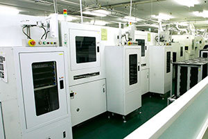
The heart: the manufacturing process for circuit boards
Let's now take a look at circuit board manufacturing operations. Hitachi prints solder paste onto its own original circuit boards which then have around 3000 components installed on them. The printing of the paste solder is performed with a solder paste printer onto which a metal mask is attached. The design of the metal mask is Hitachi's own and it has a range of opening shapes including square, triangular, baseball home plate and more depending on the component in question.
The reason for this is the range of large, medium-size, and small components that are combined on circuit boards and the great variety of differently shaped components to which the solder is applied. In order to securely attach the approximately 3000 components to the circuit board under these conditions a range of sizes and shapes of openings must be provided to suit each and every component.
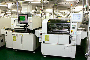
Paste printers
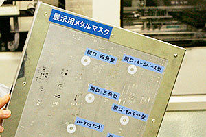
Metal mask
A reflow oven featuring a nitrogen atmosphere is used during the soldering process due to the risk of oxidization.Heat is then applied, but in order to avoid putting the components under stress, the heat is applied in small increments at the lowest possible temperature and it is regulated to minimize damage to components.
Once soldering is finished, a 3D x-ray solder surface check device is used to inspect the state of the solder. This means that x-rays are applied to the solder and the resulting image is used to detect defects. The standards for inspection are rigorous, and if the solder is even slightly raised or out of place then it is picked up here.

Reflow oven
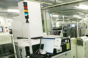
3D x-ray solder surface check device
However, for sections in which inspection values are set high, areas that are soldered to within in a permitted range of error are also flagged up so such places are always ultimately subject to a visual check by human eyes.
In some cases components are attached without solder. To embed these components, a press fit that can deliver a maximum force of five tons is used, and the amount of pressure is adjusted based on the thickness and length of the pins.
Press fit
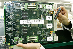
These kinds of components are embedded on circuit boards using the press fit.
